74170, NTE74170
- Category: TTL 74 series
- Sub Category: Registers
- Manufacturer: NTE electronics
Short Description
TTL − 4−by−4−Register File with Open Collector Outputs.
General Description
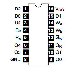
The NTE74170 is a 4−by−4 register with open collector outputs in a 16−Lead plastic DIP type package incorporating the equivalent of 98 gates. The register file is organized as 4 words of 4 bits each and separate on−chip decoding is provided for addressing th four word locations to either write−in or retrieve data. This permits simultaneous writing into one location and reading from another word location</br>Four data inputs are available which are used to supply the 4−bit word to be stored. Location of the word is determined by the write−address inputs A and B in conjunction with a write−enable signal. Data applied at he inputs should be in its true form. That is, if a high−level signal is desired from the output, a high level is applied at the data input for that particular bit location. The latch inputs are arranged so that new data will be accepted only if both internal address gate inputs are high. When this condition exists, data at th D input is transferred to the latch output. When the write−enable input, GW, is high, the data inputs are inhibited and heir levels can cause no change in the information stored in the internal latches. When the read−enable input, GR, is high, the data outputs are inhibited and remain high.</br>This arrangement — data−entry addressing separate from data−read addressing and individual sense line — eliminates recovery times, permits simultaneous reading an writing, an is limited in speed only by the write time (30 nanoseco</br>All inputs are buffered to lower the drive requirements to one TTL standard load. Input−clamping diodes minimize switching transients to simplify system design. High=speed, double−ended AND−OR− INVERT gates are employed for the read−address function and drive high−sink−current, open−collector outputs. Up to 256 of these outputs may be wired−AND connected for increasing the capacity up to 1024 words. Any number of these registers may be paralleled to provide n−bit word length.
Features
•Separate Read/Write Addressing Permits Simultaneous Reading and Writing</br>•Fast Access Time: 20ns (Typ)</br>•Organized as 4 Words of 4 Bits</br>•Expandable to 1024 Words of n−Bits.
Applications
•Scratch−Pad Memory</br>•Buffer Storage between Processors</br>•Bit Storage in Fast Multiplication Designs.
Absolute Maximum Rating
>Supply Voltage, V<sub>CC</sub>.... 7V</br> >DC Input Voltage,V<sub>IN</sub>...5.5V</br> >Off−State Output Voltage. . . 5.5V>/br> >Operating Temperature Range, TA.... 0°C to +70°C</br> >Storage Temperature Range, Tstg... −65°C to +150°C
Datasheet Link
http://datasheet.octopart.com/NTE74170-NTE-Electronics-datasheet-22128720.pdf